Guide to Memory Engineering
Physics, Fabrication, and System Design
1 Purpose
This document explores the engineering and manufacturing of digital memory. You will learn about the lifecycle of memory, from the underlying physics of DRAM and NAND cells to the complex fabrication processes and architectural trade-offs required to build modern, high-performance memory and storage devices.
2 What You’ll Learn
By the end of this reading, you will be able to:
- Differentiate between the core memory technologies: SRAM, DRAM, and NAND Flash.
- Describe the physical structure of a DRAM and a NAND Flash memory cell.
- Explain why the memory industry shifted from 2D to 3D NAND manufacturing.
- Distinguish between different memory module types like UDIMM, RDIMM, and LRDIMM.
- Explain the architectural differences between system RAM (DDR) and video RAM (GDDR).
This reading maps to the following program and course learning outcomes:
- Program Learning Outcomes (PLOs):
- 3. Apply terminology and numeric or system concepts: This document covers deep technical terms like 1T1C, 3D NAND, FTL, ECC, RDIMM, and GDDR, which are critical systems-level concepts.
- Course Learning Outcomes (CLOs):
- 1. Identify hardware and basic network components: This provides a deep dive into the physical construction and engineering of memory and storage hardware.
- 3. Troubleshoot hardware and basic network components: Understanding NAND types, wear-leveling, and ECC is crucial for selecting appropriate storage and diagnosing failures.
This exercise will help you develop the following skills and knowledge, which align with the O*NET SOC Code 15-1232.00 for Computer User Support Specialists.
| Learning Objective | O*NET KSAs | Technologies Used |
|---|---|---|
| Differentiate between volatile and non-volatile memory. | Knowledge: Computers & Electronics Skills: Reading Comprehension Abilities: Information Ordering |
N/A (Conceptual) |
| Explain the fundamental trade-offs in memory design. | Knowledge: Computers & Electronics Skills: Critical Thinking |
N/A (Conceptual) |
| Explain why a high-endurance SSD requires a DRAM cache. | Knowledge: Computers & Electronics Skills: Systems Analysis, Troubleshooting Abilities: Problem Sensitivity |
Solid State Drives (SSDs) |
3 An Overview of Memory Engineering
Digital memory forms the foundational layer of the computing hierarchy. Engineering this memory involves deep trade-offs between speed, density, power consumption, and manufacturing complexity. This document delves into these complexities, from the fundamental physics of memory cells to the sophisticated fabrication processes required to create modern memory devices.
3.1 Core Memory Technologies
| Type | Volatility | Primary Function | Key Characteristic |
|---|---|---|---|
| SRAM (Static RAM) | Volatile | CPU Caches (L1, L2, L3) | Extremely fast; relies on a 6-transistor cell; low density. |
| DRAM (Dynamic RAM) | Volatile | System Main Memory (RAM) | High density; relies on a 1-transistor/1-capacitor cell; requires constant refresh. |
| NAND/NOR Flash | Non-Volatile | Storage (SSDs, Firmware) | Data is retained when powered off; uses floating-gate transistors. |
3.2 The Physics of a Memory Cell
- DRAM Cell (1T1C): Consists of a single access transistor and a storage capacitor. The capacitor holds a tiny electrical charge, representing a ‘1’ (charged) or a ‘0’ (discharged). Because this charge leaks, DRAM requires a constant “refresh” operation.
- NAND Flash Cell: Uses a Floating-Gate Transistor, which traps electrons in an electrically isolated layer to store data. By storing varying amounts of charge, multiple bits can be encoded per cell (e.g., MLC, TLC, QLC), drastically increasing density at the cost of speed and endurance.
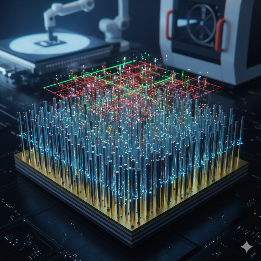
4 From 2D to 3D: Modern Memory Fabrication
As manufacturers tried to shrink 2D NAND flash, they hit a physical limit where cells were so close together they began to interfere with each other. The solution was to go vertical, stacking memory cells in skyscraper-like arrays. This technology, known as 3D NAND or V-NAND, allows for massive increases in density.
Error: Video with ID "KCWDzWG1BcI" not found in document metadata. This may be because the shortcode is being used in an unsupported context, such as a listing page.
5 System-Level Design and Specialized Memory
5.1 Engineering for a Workload: Consumer vs. Enterprise
The performance and endurance of a storage device are dictated by its intended workload.
- Low-Tier (e.g., USB Flash Drive): Engineered for sequential file transfers. They often use low-endurance QLC NAND (4 bits per cell) and lack a DRAM cache, making them slow for the random I/O operations required by an operating system.
- High-Tier (e.g., M.2 NVMe SSD): Engineered for demanding random I/O (booting an OS, running databases). They use higher-endurance TLC or MLC NAND, a dedicated DRAM cache to speed up data lookups, and a powerful controller chip that performs wear-leveling to distribute writes evenly and prevent premature failure.
5.2 Reliability and Error Correction (ECC)
Error-Correcting Code (ECC) memory is used in servers and workstations to ensure data integrity. It uses extra bits and an algorithm (like a Hamming code) to detect and correct single-bit errors on the fly. ECC requires support from the memory module, CPU, and motherboard.
- UDIMM (Unbuffered DIMM): Standard consumer RAM. Data travels directly from the memory controller to the RAM chips.
- RDIMM (Registered DIMM): Used in servers. Includes a register chip on the module to buffer signals, reducing electrical load on the memory controller and allowing for much larger total memory capacities.
- LRDIMM (Load-Reduced DIMM): Used in high-capacity servers. Buffers both data and command signals to allow for the maximum possible memory density.
5.3 Bandwidth vs. Latency: VRAM for Graphics
Video RAM (VRAM) is specialized memory used by a Graphics Processing Unit (GPU). It uses technologies like GDDR (Graphics Double Data Rate), which is architecturally different from the DDR RAM used for the main system.
- Key Difference: VRAM is optimized for maximum bandwidth over a very wide memory bus (e.g., 256-bit or 384-bit). System RAM is optimized for low latency over a narrower bus (typically 64-bit).
- Use Case: The massive bandwidth of VRAM is essential for feeding the thousands of GPU cores with the data needed for parallel tasks like graphics rendering, AI model training, and scientific computing.
5.4 Packaging and Evolution
- Packaging: The raw memory die is packaged into a form that can be used in a computer. This has evolved from individual DIP chips soldered to the board, to SIMM modules, to the modern DIMM (Dual In-line Memory Module) standard used today. SO-DIMMs are a smaller version for laptops.
- DDR Evolution: The evolution from DDR1 to DDR5 is driven by the need for more speed at lower power. Each generation increases the data rate and lowers the operating voltage (e.g., DDR4 at 1.2V vs. DDR5 at 1.1V).
6 Reflect and Review
Now that you have reviewed this document, take a moment to reflect on your learning. In your Microsoft Teams Student Notebook, create a new page for this topic and write down the following:
- 3 different types of memory modules (e.g., UDIMM, RDIMM).
- 2 reasons VRAM is architected differently from system RAM.
- 1 question you still have about how ECC memory works.
This reflection is for your instructor to review and helps solidify your understanding of the concepts.
Test your understanding with the following questions. These questions provide retrieval practice and reinforce key concepts covered in this reading. In your Microsoft Teams Student Notebook, answer the following:
- What is the fundamental physical difference between a DRAM cell and a NAND flash cell?
- What critical manufacturing problem did 3D NAND technology solve?
- What is the purpose of a DRAM cache on a high-end SSD?
- What is the main difference between an RDIMM and a standard UDIMM?
- Why is high bandwidth more important than low latency for VRAM?