Memory Manufacturing and Engineering Design
Physics, Fabrication, and Architectural Trade-offs
Digital memory forms the foundational layer of the computing hierarchy, serving as the volatile and non-volatile workspace for the CPU. Engineering memory involves deep trade-offs between speed, density, power consumption, and manufacturing complexity. This document delves into these complexities, starting with the basic principles of memory physics and transitions from defining the fundamental memory types to detailing the sophisticated semiconductor processes and architectural decisions required to create modern Integrated Circuit (IC) memory.
1 The “What”: An Overview of Memory Types
Memory technologies are broadly categorized based on their volatility (whether data is retained without power) and access speed.
| Type | Volatility | Primary Function | Key Characteristic |
|---|---|---|---|
| SRAM (Static RAM) | Volatile | CPU Caches (L1, L2, L3) | Extremely fast; relies on a 6-transistor cell; low density. |
| DRAM (Dynamic RAM) | Volatile | System Main Memory (RAM) | High density; relies on a 1-transistor/1-capacitor cell; requires constant refresh. |
| NAND/NOR Flash | Non-Volatile | Storage (SSDs, Firmware) | Data is retained when powered off; uses floating-gate transistors; slower write/erase cycles. |
2 The Physics of Storage: Core Cell Structure
The manufacturing and design complexity of a memory IC is defined primarily by its core storage cell. Miniaturization drives innovation, forcing engineers to adopt three-dimensional structures.
2.1 Dynamic Random Access Memory (DRAM) Cell
The fundamental DRAM cell consists of a single access transistor and a single capacitor (1T1C).
Access Transistor (MOSFET): Acts as a gate, controlled by the Wordline (WL), to connect or disconnect the storage capacitor from the Bitline (BL).
Storage Capacitor: Holds a tiny electrical charge, representing a ‘1’ (charged) or a ‘0’ (discharged). Charge leakage necessitates the “refresh” operation every few milliseconds.
As lithographic nodes shrink, the planar area available for the capacitor decreases, which reduces capacitance. To maintain the required charge (for signal integrity and noise immunity), manufacturers utilize 3D structures:
Stacked Capacitors: The capacitor is built vertically above the transistor.
Trench Capacitors: The capacitor is built downward into a deep hole etched into the silicon substrate.
2.2 NAND Flash Memory Cell
Flash memory uses a Floating-Gate Transistor (FGT), which is fundamentally a standard MOSFET with an extra, electrically isolated conducting layer (the floating gate) sandwiched between the control gate and the silicon channel.
Programming (Writing): Electrons are forced onto the floating gate via Fowler-Nordheim tunneling or Hot-Electron Injection.
Storage: The trapped charge on the floating gate permanently shifts the transistor’s threshold voltage (\(V_{th}\)). A subsequent read operation measures this \(V_{th}\) to determine the stored state.
Multi-Level Cells (MLC, TLC, QLC): By storing varying amounts of charge, multiple bits (2, 3, or 4) can be encoded per cell, drastically increasing density at the cost of slower speeds and reduced endurance.
3 Semiconductor Manufacturing and Fabrication
The fabrication of memory ICs requires the most aggressive lithography techniques due to the immense density required (billions of cells on a single die).
3.1 DRAM Fabrication Challenges
The most challenging step in DRAM fabrication is creating the high-aspect-ratio 3D capacitor structures:
Atomic Layer Deposition (ALD): Critical for depositing ultra-thin, high-k (high dielectric constant) materials within the complex 3D structures (trenches or stacks). This maximizes capacitance while minimizing physical space.
Patterning: Achieving the required precision for the transistor gates and capacitor landings, often pushing deep into Extreme Ultraviolet (EUV) lithography domains. Misalignment of even a few nanometers can cause catastrophic cell failure.
3.2 Flash Fabrication: The Move to 3D NAND
Scaling planar (2D) NAND hit a physical limit due to cell-to-cell interference and voltage coupling. Modern Flash manufacturing overcame this challenge by moving to 3D NAND (or V-NAND) technology, stacking memory cells vertically in a skyscraper-like array.
The fabrication process for 3D NAND is complex and relies heavily on precision deposition and etching techniques:
Alternating Layer Deposition: Hundreds of thin layers of material (alternating between a conductive, temporary sacrificial layer, and the insulating silicon oxide layer) are deposited onto the silicon wafer. This forms the foundation of the vertical stack.
High-Aspect Ratio (HAR) Etching: This is the most critical and difficult step. Using reactive ion etching (RIE), tiny, deep channel holes are etched through the entire stack of alternating layers. As layer counts increase (from 64L to 232L+), the aspect ratio (depth-to-width) becomes immense, requiring advanced plasma etch control to maintain verticality and uniformity.
Gate/Wordline Formation (Staircase Etching): After the initial etch, the sacrificial layers are removed, and the resulting cavities are filled with conductive material (typically Tungsten) to form the Wordlines (WLs). A separate staircase-like etch process is used on the side of the stack to expose the ends of the WLs, allowing for electrical connection and addressing.
Charge-Trap Flash (CTF) Structure: Unlike the floating conductive gate of 2D NAND, 3D NAND utilizes Charge-Trap Flash (CTF). The channel hole is lined with a specific ONO (Oxide-Nitride-Oxide) stack:
The inner oxide acts as the tunneling barrier.
The silicon nitride layer acts as the charge-trapping material.
The outer oxide acts as the blocking layer.
This structure stores charge in a layer of silicon nitride rather than a floating conductive gate. CTF is inherently easier to manufacture in 3D stacks, offers better endurance, and is more resistant to charge loss from neighboring cells (eliminating the interference problem that killed 2D scaling).
Author: Asianometry | View Channel
An overview of memory engineering, including the physics behind different types of memory, semiconductor manufacturing challenges, and architectural considerations.
4 Memory IC Architecture and Organization
A memory IC is not just a grid of cells; it is a highly organized parallel processing machine.
4.1 Internal Organization
The core memory array is divided into Banks, allowing multiple access operations to occur simultaneously. Data access follows a two-step process:
Row Access (Wordline Activation): The Row Address Strobe (RAS) signal selects a Wordline (WL) via the Row Decoder. This activates an entire row of memory cells (typically thousands of bits).
Column Access (Bitline Selection): Activating the WL dumps the minute charges onto the Bitlines (BL). The Column Address Strobe (CAS) signal then selects specific Bitlines via the Column Decoder, directing the desired data out.
4.2 Sense Amplifiers
The data stored in a DRAM capacitor is incredibly small (femtofarads, fF). A Sense Amplifier is the circuit required to detect and amplify this minute differential voltage between a cell’s bitline and a reference bitline. Sense amps are crucial: they must amplify the signal in microseconds and simultaneously rewrite the data back into the capacitor, fulfilling the necessary refresh cycle for the accessed row.
5 Engineering Design and Trade-offs
Memory engineering involves balancing competing physical constraints—a process known as the “Iron Triangle” of speed, power, and density.
5.1 Design Trade-offs
Density vs. Speed: Increasing density (smaller cells) leads to lower capacitance, weaker signals, and longer stabilization times for the sense amplifiers, which ultimately limits clock speed.
Speed vs. Power: To increase speed, signals must transition faster, requiring more current and higher operating voltages (though standards trend toward lower voltage). High-speed I/O drivers also contribute significantly to power draw.
5.2 Error Correction Code (ECC)
ECC is a mandatory feature for all mission-critical (server/data center) DRAM modules. Due to high density, DRAM cells are susceptible to soft errors (spontaneous bit flips caused by cosmic rays or local leakage).
ECC uses a specific number of parity bits (typically 8 extra bits for every 64 data bits) to generate a unique digital signature for the data. The most common implementation uses Hamming codes, which can:
Detect double-bit errors.
Correct single-bit errors.
5.3 Durability and Resilience: Storage Device Tiers
The performance and endurance disparity between a simple consumer USB flash drive and a high-end M.2 NVMe Solid State Drive (SSD) is a critical engineering distinction driven by intended workload requirements.
| Component/Feature | USB Flash Drive (Low-Tier) | M.2 NVMe SSD (High-Tier) |
|---|---|---|
| Workload | Sequential (file transfer, storage) | Random I/O (OS boot, VM disk, databases) |
| NAND Type | Often QLC (Quad-Level Cell) or TLC | Primarily TLC (Triple-Level Cell) or higher-grade MLC |
| Controller | Simple, low-power, single-core | Multi-core, high-performance, complex firmware |
| DRAM Cache | Rarely present (DRAM-less) | Dedicated DDR SDRAM for FTL mapping |
| Wear Management | Basic static/dynamic wear leveling | Advanced, distributed wear-leveling algorithms & Over-Provisioning (OP) |
Workload Differentiation: A low-cost flash drive is engineered for simple, sequential writes (e.g., copying a large video file) and infrequent, moderate reads. Longevity and random access speed are secondary. They often use low-endurance QLC NAND, storing four bits per cell, which sharply reduces the number of program/erase (P/E) cycles the cell can sustain (sometimes \(\approx 1,000\) cycles).
In contrast, a boot drive or a VM disk must handle intensive, small-block Random I/O operations—the continuous reading, writing, and rewriting of metadata, logs, and small system files. This demanding workload requires:
DRAM Cache: High-tier SSDs include a separate DRAM module to rapidly store the Flash Translation Layer (FTL) mapping table. This map tells the controller where every logical block of data resides physically in the NAND, dramatically speeding up random access.
Advanced Controllers: These multi-core processors execute sophisticated Wear-Leveling algorithms, ensuring data blocks are written evenly across the entire NAND array to prevent premature failure of any single block.
Over-Provisioning (OP): High-end SSDs reserve 7% to 28% of the total physical space as invisible OP. This buffer gives the wear-leveling algorithms ample spare blocks to swap out failing cells and maintain sustained performance during heavy writes, which is mandatory for resilient operating system usage.
Therefore, while an external NVMe drive uses a high-speed USB interface for transport, its internal durability and resilience are dictated by its SSD architecture (controller, DRAM, and wear management) designed specifically for the demanding random I/O of persistent computing.
5.4 Packaging: From Die to DIMM
The raw memory die is packaged into a BGA (Ball Grid Array) and then mounted onto a standardized module:
DIMM (Dual In-line Memory Module): Standard for desktop/server applications.
SO-DIMM (Small Outline DIMM): Used in laptops and small form factor devices.
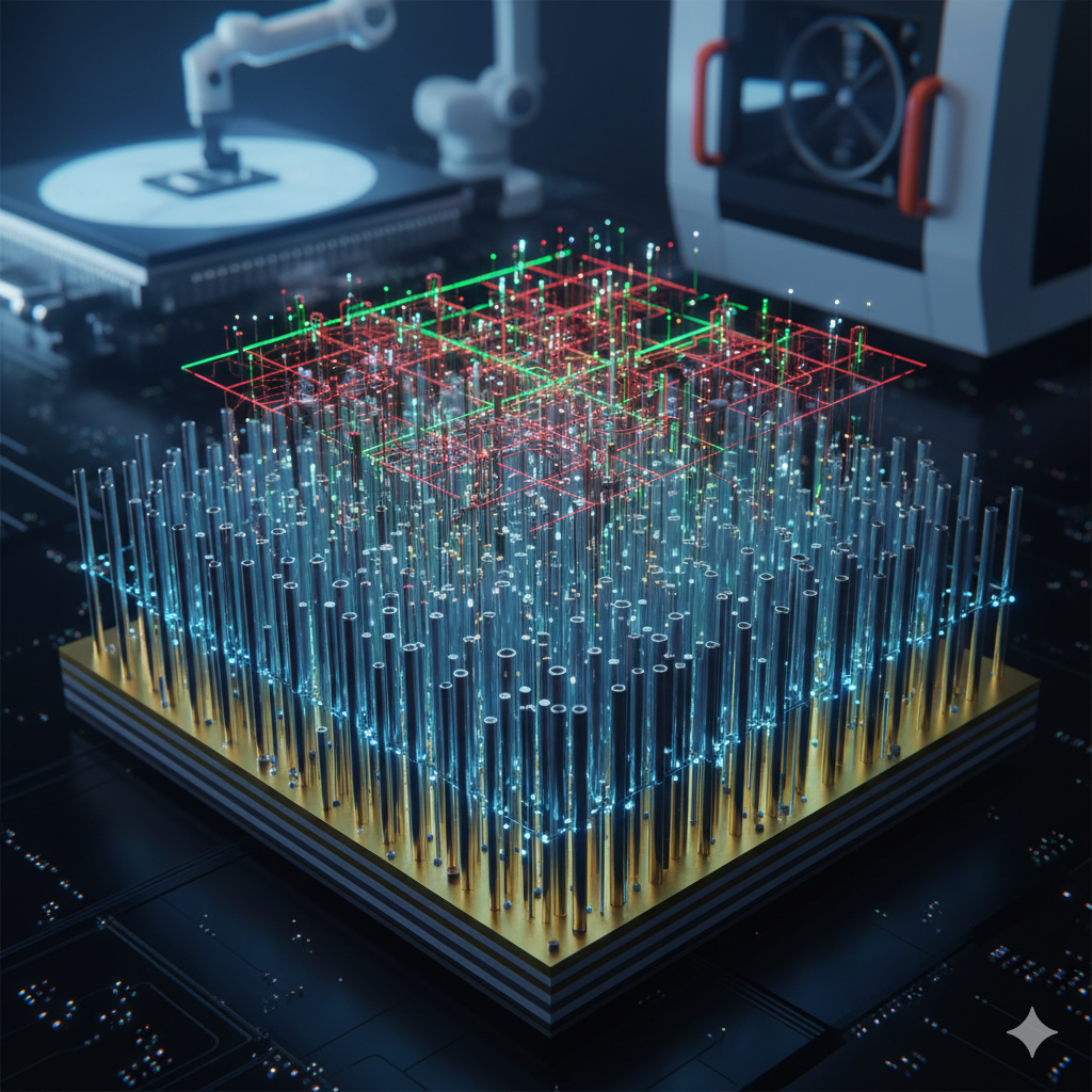
HBM (High Bandwidth Memory): An advanced packaging technology where DRAM dies are vertically stacked and connected via through-silicon vias (TSVs) directly next to the CPU/GPU, enabling unprecedented bandwidth for AI and graphics workloads.
6 Standards Evolution and Future Directions
6.1 DRAM Standard Evolution (DDR)
The evolution from DDR1 to the latest DDR5 is primarily driven by three metrics:
Data Rate (Speed): Achieved through higher clocking frequencies and improved signal integrity techniques.
Prefetch Buffer Size: DDR standards increase the amount of data fetched per clock cycle. (DDR1/2N prefetch, DDR4 8N prefetch, DDR5 16N prefetch).
Voltage: Each generation lowers the operating voltage (e.g., DDR3 at \(1.5V \rightarrow\) DDR5 at \(1.1V\)), significantly reducing overall power consumption.
DDR5 also introduced two independent 32-bit channels per module, improving access efficiency over the single 64-bit channel of previous generations.
6.2 Flash Technology Types
While both are non-volatile, their architecture dictates their use:
NOR Flash: The memory cells are connected in parallel, allowing for random-access read operations (like DRAM/SRAM). Ideal for storing firmware and bootloaders where fast, random reads are essential.
NAND Flash: Cells are connected in series, which makes random reads slow but sequential access highly efficient. This architecture is necessary for high density and is the foundation for all modern SSDs and USB drives.