Computer memory is the essential component that stores data and instructions for immediate and future use, acting as the bridge between the processor and storage. It is arguably the most critical subsystem governing a computer’s overall performance. This article provides a technical introduction to the primary types of memory, their historical evolution, modern architectures, and how they integrate to support process execution.
Memory Hierarchy and Core Types
Modern computing utilizes a memory hierarchy—a structure that organizes memory based on speed, capacity, and cost. Faster, smaller, and more expensive memory is closer to the CPU, while slower, larger, and cheaper memory is further away.
Primary Memory: Volatility and Core Types
The two fundamental classes of primary memory, Random-Access Memory (RAM) and Read-Only Memory (ROM), are distinguished fundamentally by their volatility—whether they retain data when power is removed.
1. Volatile Memory (RAM)
RAM is the working memory of the computer, used to store data and instructions for programs that are currently running. It is volatile, meaning its contents are lost when the power is turned off.
Dynamic RAM (DRAM): The most common type of RAM, used for the main system memory. DRAM stores each bit of data in a separate capacitor within an integrated circuit. Since capacitors leak charge, DRAM needs to be periodically refreshed (hence “dynamic”) to maintain the data.
Synchronous DRAM (SDRAM): A significant advancement over earlier Asynchronous DRAM. SDRAM is synchronized to the clock speed of the CPU, which allows it to process instructions more efficiently and predictively.
Double Data Rate SDRAM (DDR SDRAM): The modern standard. DDR transfers data on both the rising and falling edges of the clock signal, effectively doubling the data rate without increasing the clock frequency. Current generations include DDR4 and DDR5, each offering increased speeds and lower power consumption than its predecessor.
Static RAM (SRAM): Used primarily for CPU Cache. SRAM stores each bit using a bistable latch (six transistors), requiring continuous power but no refresh cycles (hence “static”). This makes SRAM much faster than DRAM, but it is also physically larger and significantly more expensive, limiting its use to small, high-speed applications.
2. Non-Volatile Memory (ROM and Flash)
ROM is non-volatile memory that contains critical boot-up instructions (like the BIOS or UEFI firmware) needed to start the computer. Data in ROM is typically written during manufacturing or during a firmware update.
Mask ROM (MROM): The original type, programmed during the semiconductor fabrication process. Data is permanent and cannot be altered.
Programmable ROM (PROM): Can be written to once by the user using a special device (a PROM programmer).
Electrically Erasable Programmable ROM (EEPROM) / Flash Memory: Can be erased and reprogrammed electrically. NAND Flash is a high-density, low-cost form of non-volatile memory that forms the basis of Solid-State Drives (SSDs), USB drives, and memory cards, effectively serving as modern secondary storage.
Advanced RAM Classes: Reliability for Workstations and Servers
While standard desktop RAM (known as Unbuffered DIMMs, or UDIMMs) prioritizes speed and low cost, enterprise-grade systems like servers and high-end workstations demand absolute data integrity and scalability. This requirement leads to the use of specialized RAM modules, primarily ECC memory.
Error-Correcting Code (ECC) Memory
ECC memory provides a mechanism to detect and correct single-bit errors that occur due to background radiation, voltage fluctuations, or manufacturing defects—phenomena sometimes referred to as “soft errors.” In mission-critical applications, such a bit flip could corrupt vital data or crash the system.
How ECC Works
Standard memory modules transfer 8 data bits for every byte. ECC modules, by contrast, use 9 bits: the 8 data bits plus an additional parity bit or check bit.
ECC uses algorithms, often based on Hamming codes, to generate a checksum for the data being written. When the data is read:
The same algorithm is applied to the retrieved 8 data bits.
The resulting checksum is compared to the stored check bit.
If they match, the data is correct.
If they mismatch, the code can not only detect the error but, in the case of a single-bit error, identify and flip the incorrect bit back to its proper state, correcting the error silently.
RAM Module Classifications for ECC
Unbuffered DIMM (UDIMM): Used in most consumer desktops. Data travels directly from the Memory Controller on the CPU to the RAM chips. UDIMMs can be non-ECC or ECC. Non-ECC UDIMMs are the most common desktop standard.
Registered DIMM (RDIMM): Primarily used in servers and high-end workstations. RDIMMs include a register chip located on the module between the DRAM chips and the system’s memory controller. This register buffers the command and address signals for one clock cycle.
- Benefit: By buffering these signals, RDIMMs reduce the electrical load on the memory controller, allowing systems to support a significantly larger number of DIMMs and much greater total memory capacity (e.g., in a multi-socket server). RDIMMs typically require ECC support.
Load-Reduced DIMM (LRDIMM): Used in high-density, extreme-capacity server environments. LRDIMMs buffer both the command/address signals and the data signals. This further reduces the electrical load on the memory controller, enabling the use of even higher-capacity modules and maximizing the total memory a server can manage.
Hardware Support for ECC
ECC functionality is not universal and requires support from three specific components:
Memory Module: The RAM stick itself must be an ECC module (having the extra chips for the check bits).
CPU: The Central Processing Unit must contain a Memory Controller capable of generating and processing the ECC check bits (e.g., many Intel Xeon and AMD Epyc processors, and specific desktop CPUs like some AMD Ryzen models, support this feature).
Motherboard/Chipset: The motherboard chipset and BIOS must be designed to enable and utilize ECC communication between the CPU and the memory slots. A motherboard designed for standard consumer UDIMMs will not recognize or utilize the ECC feature, even if an ECC module is installed.
Specialized Memory: Video RAM (VRAM) and GPGPU Computing
Video Random-Access Memory (VRAM) is specialized memory dedicated to the Graphics Processing Unit (GPU). It utilizes specialized technologies like Graphics Double Data Rate (GDDR) SDRAM and is architecturally distinct from system DRAM, focusing on extreme throughput to handle the massive parallel data requirements of modern computing.
VRAM vs. System DRAM: Bandwidth for Parallelism
The primary distinction between system RAM (DDR) and VRAM (GDDR) lies in their architectural optimization for the specific tasks of the CPU versus the GPU.
| Primary Goal |
Low latency, moderate bandwidth |
Maximum bandwidth, high throughput |
| Data Bus Width |
Typically 64 bits per channel (or 128 bits total for standard configurations) |
Very Wide Bus (256-bit, 384-bit, or even 4096-bit for HBM) |
| Connection |
Modular DIMMs connecting to the CPU via the Memory Controller |
Chips soldered directly to the GPU’s printed circuit board (PCB) |
| Optimized For |
Sequential data access, CPU processes |
Massive parallel data access (simultaneous reads/writes) |
The Significance of the Wide Bus for Tensors
GDDR memory chips are connected to the GPU via an extremely wide memory bus (e.g., 256-bit or 384-bit compared to DDR’s standard 64-bit channel). This bus width is critical because it allows the GPU to move huge chunks of data simultaneously, maximizing bandwidth.
This architecture is vital for matrix manipulations and tensor processing, which form the foundation of both graphics rendering and AI workloads:
Graphics Processing: Rendering involves manipulating vast matrices of color, depth, and vector data (primitives, textures, etc.). A wide VRAM bus allows the GPU’s thousands of cores to quickly access the necessary texture and geometry data, ensuring the high-resolution frame buffer is filled rapidly and without bottleneck.
Tensor Computing (AI/ML): In deep learning, data is represented as multi-dimensional arrays called tensors. Training neural networks requires billions of rapid matrix multiplications. The VRAM’s wide bus is essential because it feeds these massive, simultaneous data arrays to the GPU cores fast enough to keep the parallel processing units fully utilized, dramatically reducing training time for complex models using frameworks like CUDA and ROCm.
Role in Graphics and Scientific Computing
Graphics Rendering: VRAM primarily serves as the frame buffer (where the final image is stored before display) and the storage location for essential assets like textures, shaders, and geometric data. Its high bandwidth ensures the GPU can continuously read and write millions of pixels and textures per second.
General-Purpose GPU (GPGPU) Computing: Modern VRAM’s extreme bandwidth is also leveraged for non-graphical parallel processing tasks in scientific computing, deep learning, and data analytics. This is accomplished through parallel programming models that allow developers to utilize the GPU’s many cores:
CUDA (Compute Unified Device Architecture): NVIDIA’s proprietary parallel computing platform and programming model, allowing developers to use the GPU’s thousands of cores for accelerating tasks like AI model training, molecular dynamics, and financial simulations.
ROCm (Radeon Open Compute Platform): AMD’s open-source equivalent platform, providing a similar environment for harnessing the massive parallel processing power of their Radeon GPUs for high-performance computing.
In GPGPU scenarios, VRAM acts as a massive, high-speed scratchpad for the GPU’s many cores, holding the input data, intermediate results, and final output of the computationally intensive task.
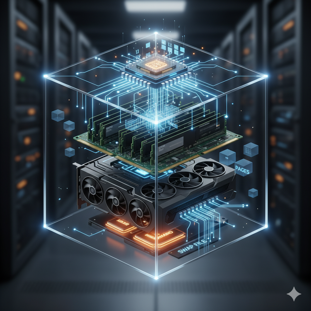
The CPU-Memory Interface and Cache Architecture
The efficiency of process execution hinges on the speed at which the CPU can access data. This is facilitated by a sophisticated cache hierarchy that utilizes SRAM.
Virtual Memory and Paging
Before data is processed by the cache and registers, the operating system manages memory using virtual memory. This technique allows the system to compensate for physical memory (DRAM) shortages by temporarily transferring blocks of data, called pages, from RAM to a designated area on the slower secondary storage (like an SSD or HDD) known as the swap file or paging file. This gives the illusion of a much larger contiguous memory space to running applications. While crucial for system stability and multi-tasking, accessing the swap file is drastically slower than accessing physical RAM, leading to a noticeable performance drop known as “thrashing.”
How Memory Feeds the CPU
\[\text{Data Access Speed: Registers} > \text{L1 Cache} > \text{L2 Cache} > \text{L3 Cache} > \text{DRAM} > \text{SSD/HDD}\]
Process Execution: When a program runs, its instructions and necessary data are loaded from secondary storage (like an SSD) into the main system memory (DRAM).
Cache Levels: The CPU needs data faster than DRAM can provide. To mitigate this memory wall (the growing performance gap between CPU and DRAM speeds), data that is likely to be needed soon is moved into the cache.
L1 Cache (Level 1): The smallest and fastest cache, integrated directly onto the CPU core. It’s split into an instruction cache and a data cache. It is the first place the CPU looks for data.
L2 Cache (Level 2): Larger and slightly slower than L1. It is often exclusive to each CPU core.
L3 Cache (Level 3): The largest and slowest of the on-chip caches, often shared across all cores on the processor die.
Registers and ALU: If the data is found in the cache (a cache hit), it’s immediately moved to the extremely fast CPU registers for processing by the Arithmetic Logic Unit (ALU). If the data is not in the cache (cache miss), the CPU must fetch it from the slower DRAM, incurring a significant delay.
The entire architecture is designed to maximize locality of reference—the tendency for a program to access memory locations that are spatially or temporally close to those it has accessed recently.
Historical Evolution and Modern Packaging
Memory has undergone radical changes, driven by the need for higher density, faster speeds, and modularity.
Historical Packages
- Dual In-Line Package (DIP or DIPP): An early package where individual memory chips were directly soldered onto the motherboard. This design was rigid and made memory upgrades difficult.
The Rise of Memory Modules
To facilitate easier upgrades and maintenance, individual chips were grouped onto standardized circuit boards, leading to the memory module:
Single In-Line Memory Module (SIMM): Used in the late 1980s and 1990s. SIMMs had connectors on one side of the board and were installed by plugging them into a slot at an angle.
Dual In-Line Memory Module (DIMM): The current standard, which superseded SIMMs. DIMMs have separate electrical contacts on both sides of the board. They offer a wider data path (typically 64 bits) and are easier to install and remove.
- SO-DIMM (Small Outline DIMM): A physically smaller version of a DIMM used in laptops, notebooks, and small form factor devices.
Advancements in Chip Architecture
The fundamental chip material remains silicon, but the internal design and interconnections have advanced dramatically:
- High Bandwidth Memory (HBM): A modern, high-performance DRAM technology. HBM chips are stacked vertically and interconnected by a short, fast interface called a silicon interposer. This technique drastically reduces the physical distance data has to travel, significantly increasing memory bandwidth and power efficiency, making it ideal for GPUs and high-end server processors.
The continuous evolution of memory architecture and packaging—from discrete DIP chips to standardized DIMMs and stacked HBM—reflects the constant pressure to overcome the limitations of distance, power consumption, and thermal management while satisfying the ever-increasing demand for faster data processing.
Back to top