flowchart TD
    A[CPU Generates Physical Address] --> B(Memory Controller Unit);
    B --> C{Decode High-Order Bits};
    C --> D["Chip Select DIMM/Chip"];
    C --> E["Rank/Bank Address"];
    D & E --> F{Send Row Address RAS};
    F --> G(Open Row Buffer - Highest Latency);
    G --> H["Send Column Address CAS"];
    H --> I["Data Read/Write at Cell"];
    I --> J(Data Sent to CPU/Cache);

    style A fill:#D0E7FF,stroke:#367C9D,stroke-width:2px
    style G fill:#FFDDDD,stroke:#CC0000
Memory Addressing and CPU Management
The Hardware-Software Interface
Details how the Memory Controller Unit and cache hierarchy manage the physical addressing, request scheduling, and high-speed translation between the CPU and the physical DRAM cells and I/O devices.
While our previous articles explored the physical engineering and manufacturing of memory, the real magic—the moment data is actually read or written—requires a sophisticated negotiation between hardware and software. This negotiation is handled primarily by the CPU and a dedicated piece of logic known as the Memory Controller Unit (MCU).
This article explores the core mechanics of how the CPU translates a conceptual request for data into a precise physical location, and how the surrounding architecture manages these high-speed transactions.
1 1. Physical Addressing: From Logical Request to DRAM Cell
For a program to access data, the CPU must generate a physical address that uniquely identifies a location in DRAM. This process involves the CPU, the Memory Management Unit (MMU, which handles virtual-to-physical translation), and the Memory Controller Unit (MCU).
The CPU, upon receiving a memory access instruction, outputs a physical address. This address isn’t just a single number; it’s a carefully encoded set of bits used by the Memory Controller to target a specific physical component within the memory subsystem.
1.1 The Address Decoding Process
The physical address is decoded hierarchically by the Memory Controller:
Chip Select (CS): A portion of the highest-order bits selects which DIMM (Dual In-line Memory Module) and which DRAM chip on that DIMM is being targeted.
Rank/Bank Address: The next set of bits selects the Rank (a set of chips accessed simultaneously) and the specific Bank (an independent sub-array within a chip) that contains the data.
Row Address (RAS): A significant block of bits is dedicated to the Row Address, which is sent over the bus first. The Row Address Select (\(\overline{RAS}\)) signal latches this address into the selected bank, opening the entire row (often 8KB in modern systems). This is the slowest part of the access.
Column Address (CAS): The remaining bits form the Column Address, which is sent next. The Column Address Select (\(\overline{CAS}\)) signal selects the precise column (the cache line or word of data) from the currently open row.
This hierarchical process is what gives DRAM its structural efficiency. Since an entire row is opened, subsequent accesses to neighboring columns in the same row (known as a row hit) are significantly faster.
2 2. The Memory Controller Unit (MCU)
The Memory Controller Unit (MCU), almost universally integrated into the CPU die in modern systems, is the brain governing the memory subsystem. Its primary functions are to translate the decoded physical address into timing signals and electrical currents required by the DRAM module.
2.1 Core Responsibilities of the MCU:
Request Scheduling: The MCU acts as a traffic cop. It queues multiple pending memory requests from various CPU cores and I/O devices. To maximize performance, it uses sophisticated algorithms (like First-Ready, First-Come, First-Served or Row-Buffer Locality) to reorder these requests, prioritizing row hits to minimize latency and improve overall Bus Utilization.
DRAM Refresh Cycles: DRAM cells store data using tiny capacitors that slowly leak charge. The MCU is responsible for ensuring data integrity by periodically triggering refresh cycles. These cycles read the charge from every row and rewrite it, preventing data loss. This compulsory overhead consumes a small, but measurable, fraction of the total memory bandwidth.
Power Management: The MCU manages various low-power states (self-refresh modes) for the DRAM chips when they are idle, balancing energy efficiency against the latency required to wake them back up for access.
Error Correction: For systems using ECC (Error-Correcting Code) memory, the MCU is responsible for generating the error detection/correction bits on writes and using them to detect and correct single-bit errors on reads.
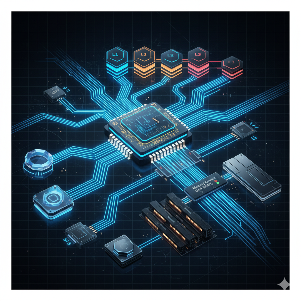
3 3. Cache Hierarchy Review
To mitigate the inherent latency of DRAM, modern CPUs employ a multi-level cache hierarchy, acting as a high-speed buffer between the CPU core and the main memory.
| Cache Level | Speed/Access Time | Size | Scope |
|---|---|---|---|
| L1 | Fastest (1-4 cycles) | Smallest (Tens of KB) | Per Core (often split into Data and Instruction) |
| L2 | Fast (10-20 cycles) | Medium (Hundreds of KB) | Per Core or Per Core Complex |
| L3 | Slower (50+ cycles) | Largest (MBs) | Shared across all Cores |
3.1 Key Concepts:
Cache Line: The smallest unit of data transfer between the cache and main memory, typically 64 bytes. When the CPU fetches a single byte, the entire 64-byte block (the cache line) containing it is moved into the cache, utilizing Spatial Locality (the idea that nearby data will soon be needed).
Cache Coherency: In a multi-core system, a single piece of data may exist in the L1 cache of multiple cores. Cache Coherency protocols (like MESI) ensure that when one core modifies the data, all other copies are immediately invalidated or updated, maintaining a single, consistent view of memory across the entire system.
Write Policies: These dictate when data written to the cache is committed back to main memory:
Write-Through: Data is written simultaneously to the cache and to main memory. This is simple and guarantees data consistency, but it is slow because every write must wait for the DRAM latency.
Write-Back: Data is written only to the cache. The cache line is marked as “dirty.” The update to main memory is deferred until the cache line is evicted (replaced by new data). This is much faster for writes but adds complexity regarding coherency and recovery.
4 4. Memory-Mapped I/O (MMIO)
The hardware-software interface extends beyond just accessing RAM. Many critical devices—like GPUs, network interfaces, storage controllers, and peripherals—need to communicate rapidly with the CPU. Memory-Mapped I/O (MMIO) is a technique that simplifies this interaction.
Instead of requiring special I/O instructions, MMIO reserves specific ranges of the CPU’s physical address space for these hardware devices. The CPU treats the device’s control registers and buffers as if they were memory locations.
When the CPU issues a read or write request to an MMIO address, the Memory Controller doesn’t send the request to the DRAM. Instead, it routes the transaction across the system bus (like the PCIe bus) to the designated peripheral device.
This approach provides several advantages:
Unified Instruction Set: The CPU uses the same load and store instructions for both memory and device access, simplifying the CPU design and compiler implementation.
Device Flexibility: The operating system can allocate or de-allocate physical address space to devices dynamically as needed.
MMIO is a prime example of the hardware-software interface at work, allowing the CPU to command the vast array of system components using the same core addressing logic it uses for RAM.
5 Conclusion
The interaction between the CPU and memory is a high-speed ballet choreographed by the Memory Controller Unit. By structuring the physical address, managing the refresh overhead, and utilizing the cache hierarchy, the system can achieve immense bandwidth and low effective latency. Understanding these mechanisms—from the physical decoding of row and column addresses to the high-level policy decisions of write-back caching and MMIO—is fundamental to grasping how a computer system effectively processes information.