Understanding the Control Unit
The CPU’s Conductor
1 The CPU’s Conductor: The Role and Function of the Control Unit
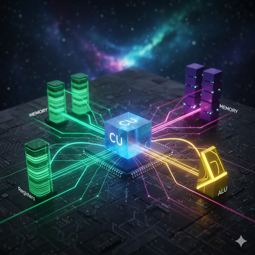
The Central Processing Unit (CPU) is often described as the brain of a computer, but within that analogy, the Control Unit (CU) is the executive function—the conductor that orchestrates the entire operation. Its fundamental purpose is to fetch instructions from memory, decode them, and generate the necessary timing and control signals required to execute the operation.
Without the CU, the Arithmetic Logic Unit (ALU) is merely a calculator, and the registers are just isolated storage bins. The CU binds these components together into a functional computing machine by managing the flow of data along the data paths.
1.1 Purpose and Core Function
The primary responsibility of the Control Unit is to manage the Instruction Cycle, often broken down into three phases: Fetch, Decode, and Execute.
1. Fetch
The CU directs the retrieval of the next instruction from main memory.
It transfers the address stored in the Program Counter (PC) to the Memory Address Register (MAR).
It asserts the
Readsignal to the memory controller.It coordinates the transfer of the data (the instruction) from the Memory Data Register (MDR) into the Instruction Register (IR).
Finally, it increments the PC to point to the next instruction.
2. Decode
The instruction, now residing in the IR, is passed to the Instruction Decoder within the CU. The decoder translates the raw binary instruction (the opcode and operands) into a sequence of micro-operations the CPU must perform. This process determines:
Which registers need to be accessed (source and destination).
Which operation the ALU must perform (add, subtract, logical AND, etc.).
Whether a memory access (read or write) is required.
3. Execute
Based on the decoded micro-operations, the CU generates the precise sequence of electrical Control Signals. These signals are binary, high-low pulses that govern every internal component, ensuring data moves correctly through the CPU’s data path at the correct clock cycle.
1.2 Interaction with Key Components
The Control Unit maintains strict control over three major areas of the CPU architecture: registers, the memory controller, and the ALU.
Interaction with Registers
The CU uses dedicated control lines to enable or disable the input (_in) and output (_out) of every register. These signals determine which register currently drives the internal bus (output enable) and which register latches the data currently on the bus (input enable).
| Register Type | CU Interaction |
|---|---|
| PC (Program Counter) | PC_out to place the next instruction address on the bus. PC_incr to update the PC value. |
| MAR/MDR | MAR_in (address to memory) and MDR_out/MDR_in (data transfer to/from memory). |
| General Purpose Registers (R1, R2, etc.) | R_i_out and R_j_in signals to select source registers for the ALU and the destination register for the result. |
Interaction with the Memory Controller
The CU acts as the sole interface for memory requests. It issues three critical signals:
Address Latch Enable: Indicates that the address currently on the bus (from MAR) is valid and should be captured by the memory controller.
Read/Write Select: A control signal specifying whether the operation is a memory read (MDR receives data) or a memory write (MDR sends data).
Wait/Ready: The CU enters a wait state upon issuing a read/write command and remains stalled until the memory controller asserts the
Readysignal, indicating the operation is complete.
Interaction with the ALU
For the ALU to perform any computation, the CU must configure its inputs and select the operation.
Input Configuration: The CU asserts signals that route data from two source registers to the ALU’s two input buffers (often called A and B registers).
Operation Selection: The CU sends a dedicated control word to the ALU, specifying the exact function (e.g.,
0001for ADD,0010for SUB,1000for AND).Output Latching: Once the ALU completes the operation (often within a single clock cycle), the CU asserts the
ALU_outsignal, enabling the result to be placed onto the internal bus, and simultaneously asserts the input signal (R_i_in) for the designated destination register.
1.3 Assembly Example: Instruction Decoding and Execution
Consider a simplified assembly instruction for a three-address register machine. This instruction adds the contents of two source registers (R2 and R3) and stores the result in a destination register (R1).
Assembly Instruction: ADD R1, R2, R3
Let’s trace the steps the Control Unit executes:
| Cycle | CU Signal Asserted | Function Performed | Instruction Phase |
|---|---|---|---|
| T1 | PC_out, MAR_in |
Transfer address of instruction from PC to MAR. | FETCH |
| T2 | Read, PC_incr |
Request instruction from memory; increment PC. | FETCH |
| T3 | Wait for memory | CU stalls until instruction is available in MDR. | FETCH |
| T4 | MDR_out, IR_in |
Move instruction from MDR into the Instruction Register (IR). | FETCH |
| T5 | Instruction Decoder (IR) | Decode ADD R1, R2, R3. The CU identifies the ADD opcode and register IDs 1, 2, and 3. |
DECODE |
| T6 | R2_out, A_reg_in |
Place data from R2 onto Bus; latch it into ALU Input A. | EXECUTE |
| T7 | R3_out, B_reg_in, ALU_Func='ADD' |
Place data from R3 onto Bus; latch it into ALU Input B; configure ALU for addition. | EXECUTE |
| T8 | ALU_out, R1_in |
Take the result from the ALU output and latch it into the destination register R1. | EXECUTE |
| T9 | Go to T1 | Cycle restarts, fetching the instruction pointed to by the new PC value. | NEXT FETCH |
This sequential, step-by-step process—timed by the system clock and controlled entirely by the Control Unit’s generated signals—is how the most abstract software instruction is translated into tangible electrical events that perform computation. The CU is, thus, the ultimate sequencer and synchronizer of the entire CPU.